


 PIC16F887 problem sa funkcijama
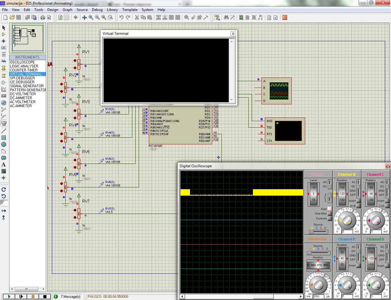
Kada zakomentarisem inisijalizaciju UART funkcije onda radi, tj imam signal PWM-a, u suprotnom ne... Evo i kod:
Code:
void Init_RS232(unsigned int baud_rate,unsigned int oscilator_MHz)
{
unsigned int baud;
unsigned long vrednost_reg;
unsigned long fcy;
//podesavanje baudrate=====================
baud=baud_rate;
fcy=oscilator_MHz*1000000;
vrednost_reg=fcy/baud/64; //formula
vrednost_reg=vrednost_reg-1; //formula
SPBRG=vrednost_reg&0x00FF; //registri za baud
SPBRGH=(vrednost_reg&0xFF00)>>8;
BRG16_bit=0; //8mo bitni baud generator
//BRGH_bit=1; //visok baud //ovo se ne sme staviti
//=========================================
//podesavanje rs232modula===================
GIE_bit=1; //globalni interrupt
PEIE_bit=1; //periferijski interrupt
SYNC_bit=0; //asinhroni mod
SPEN_bit=1; //omogucuje serijski modul;
//podesavanje transmitera==================
//TXIE_bit=1; //omogucen interrupt za TX
TXEN_bit=0; //onemoguceno slanje
//======================================
//podesavanje prijemnika================
RCIE_bit=1; //omogucen RX interrupt
CREN_bit=1; //omogucuje recivera
//=======================================
RCIF_bit=0; //================dodato====================
TXIE_bit=1; //================dodato====================
}
unsigned char RS232_Read(void)
{
unsigned char read_buf;
read_buf=RCREG;
CREN_bit=1;
return read_buf;
}
void RS232_Write(unsigned int podatak)
{
unsigned char prijem;
prijem=podatak;
TXREG=podatak;
Delay_ms(10);
TXEN_bit=1;
Delay_ms(10);
TXEN_bit=0;
TXREG=0;
}
//====== Inicijalizacija SPI ===============================================================================/
void Init_SPI(void)
{
SSPCON=0x20; //omogucen SPI i takt je Fosc/4
SSPSTAT=0x00;
SSPSTAT.BF=0; //pin koji se setuje kada je bafer pun
TRISC.B5=0; //SD0 izlazni
TRISC.B3=0; //SCK izlazni
TRISC.B4=0; //SDI ulazni
}
void Upis_SPI(char data_SPI)
{
SSPCON=0x20;
SSPBUF=data_SPI;
SSPCON=0x00;
}
//====Inicijalizacija PWM-a ===============================================================================/
void PWM1_Init(unsigned int PWM_frekvencija_Hz,unsigned char Frekvencija_oscilatora_MHz){
unsigned int fre;
unsigned char osc;
unsigned char perioda;
unsigned int obrada;
unsigned int ispuna;
osc=Frekvencija_oscilatora_MHz;
fre=PWM_frekvencija_Hz;
if(fre<620) fre=620;
if(fre>4800) fre=4800;
T2CON=0b00011010; //pres 16, pos 4
perioda=(osc*3906/(fre)); //perioda PWM signala
perioda=(perioda*4)-1;
PR2=perioda;
TMR2=0;
//GIE_bit=1;
//PEIE_bit=1;
//TMR2IE_bit=1;
TMR2IF_bit=0;
CCP1CON=0x0C; //PWM mod, ne invertovan
ispuna=0; //inicijalno ugasen PWM
obrada=ispuna; //popunjavanje registara
ispuna=ispuna&0x03;
ispuna=ispuna<<4;
CCP1CON=0x0C|ispuna;
CCPR1L=obrada>>2;
TRISC.B2=0;
PORTC.B2=0;
TMR2ON_bit=1;
}
void PWM1_Set_Parameters(unsigned int Frekvencija_Hz,unsigned char Procenat_ispune,unsigned char Frekvencija_oscilatora_MHz){
unsigned int fre;
unsigned char osc;
unsigned int perioda;
unsigned int rezolucija;
unsigned char osnova;
unsigned char dodavanje;
unsigned int ispuna_max;
unsigned int ispuna;
unsigned int max;
unsigned int obrada;
unsigned char procenat;
osc=Frekvencija_oscilatora_MHz;
fre=Frekvencija_Hz;
if(fre<620) fre=620;
if(fre>4800) fre=4800;
procenat=Procenat_ispune;
perioda=(osc*3906/(fre));
perioda=(perioda*4)-1;
PR2=perioda;
rezolucija=(log10(4*(perioda+1))/log10(2))*10;
osnova=rezolucija/10;
dodavanje=rezolucija%10;
switch (osnova){
case 6: ispuna_max=64; break;
case 7: ispuna_max=128; break;
case 8: ispuna_max=256; break;
case 9: ispuna_max=512; break;
}
switch (dodavanje){
case 1: max=ispuna_max*1.07177; break;
case 2: max=ispuna_max*1.14869; break;
case 3: max=ispuna_max*1.23144; break;
case 4: max=ispuna_max*1.31951; break;
case 5: max=ispuna_max*1.41421; break;
case 6: max=ispuna_max*1.51571; break;
case 7: max=ispuna_max*1.62450; break;
case 8: max=ispuna_max*1.74110; break;
case 9: max=ispuna_max*1.86607; break;
}
ispuna=procenat*max/100;
obrada=ispuna;
ispuna=ispuna&0x03;
ispuna=ispuna<<4;
CCP1CON=0x0C|ispuna;
CCPR1L=obrada>>2;
}
void main() {
OPTION_REG=0;
INTCON=0;
ANSEL=0;
ANSELH=0;
TRISA=255;
PORTA=0;
TRISB=0;
PORTB=0;
I2C1_Init(100000); // initialize I2C communication
Delay_ms(100);
//Init_RS232(9600,10);
Delay_ms(100);
Init_SPI();
Delay_ms(100);
PWM1_Init(800,10);
Delay_ms(100);
PWM1_Set_Parameters(800,20,10);
Delay_ms(100);
while(1){
}
}